FXP Overview
FXP is a universal solution, designed for systems generally built
on the FPGA ICs. The protocol solves the following fundamental tasks:
- Back-plane design support (back-plane, control cell, additional cells);
- Independent configuration process for any FPGA located on any cell in the device;
- High-speed data transfer between any FPGA in the system and PC;
- Real time data stream support;
The protocol consists of three levels: physical, logical and program one. Physical level
defines the device architecture and transfer medium for the connections on
cells, cross-connections and between PC and device. Logical level defines types
and structure of the packets to be transferred and their processing algorithms.
The program level defines driver and user DLL interfaces.
Designed implementation of the protocol has following features:
- Connection between PC and device - USB1.1/2.0;
- Up to seven geographically addressed cells (cards) in each device;
- Up to 16 accessed FPGAs on each cell (card);
- Independent configuration process for any FPGA of Xilinx® Virtex®/E/II/, Spartan®II/IIE/III family located on any cell in the device;
- Read/write operations for any FPGA in the device with up to 60MBps throughput;
- Real time data stream support;
- Graphical user interface with hardware part of the system, Windows® NT5 (2K/XP/Server 2003), Windows® 98/ME operating systems are supported;
- PnP technology;
- Hardware interrupts request handling;
Physical Level
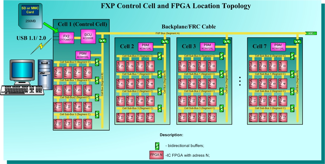
Figure 1 shows the supported by protocol design architecture.
Figure 1
Protocol supports two operation modes:
- Stand-alone mode. In the case instruction sequence for initialization is read from the FLASH card;
- PC interaction mode;
In the latter case the packets which include cell address, FPGA address,
overhead information and data are formed on the OS driver level.
Then they are transferred through USB to FX2 controller.
Packet processing is performed in DCU (Data Control Unit), and then the
data is asserted on the multiplexed data/address bus.
To provide control over line impedance, decrease capacitive loading bus
the control lines are divided into segments A, B and C
(necessity of this solution was proved by modeling). Cell addresses,
target FPGA address decoding and segment multiplexing
are performed in PBM (Process Bus MUX) chip.
Target FPGA Interface and Addressing.
Target FPGA interface consists of lines listed in the following table:
|
Signal Name1
|
Direction, I/O
|
Description
|
|
Data Transfer:
|
|
DATA[15:0]
|
I/O
|
Data/address bus
|
|
nPAEN
|
I
|
Address strobe
|
|
nWREN
|
I
|
Read strobe
|
|
nRDEN
|
I
|
Write strobe
|
|
PFULL
|
O
|
Write (FIFO full flag in stream modes of operation)
|
|
PEMPTY
|
O
|
Read acknowledgement (FIFO empty flag in stream modes of operation)
|
|
nCE
|
I
|
Chip Enable
|
|
nRESET*
|
I
|
Process Reset
|
|
PERROR*
|
O
|
Process Error (word lose in stream modes of operation)
|
|
CLK
|
I
|
Clock
|
|
Interrupt request:
|
|
nINT
|
O
|
Interrupt Request
|
|
FPGA Configuration Process (SelectMap mode)2:
|
|
nCS
|
I
|
Chip Select (while configuration process)
|
|
nPROGRAM
|
I
|
Resets configuration
|
|
RNW*
|
I
|
RW strobe
|
|
DONE*
|
O
|
Configuration process completed
|
|
nINIT*
|
O
|
Erasing of the configuration memory
|
|
CCLK
|
I
|
Clock (while configuration process)
|
- The lines, marked with (*) are optional.
- DATA[7:0] bus is also used while configuration process.
|
The strobes listed above correspond to the strobes of the FIFO.
Thus from the external interface point of view, the target FPGA
represents the set of addressed FIFO buffers. But in the FPGA
these blocks can perform any tasks including different from FIFO
since their internal interface is not specified by the protocol.
The blocks, the address corresponds to,
are referred to as "processes". Thus the full address consists
of the following fields:
- Cell address (3 bits);
- Target FPGA address (5 bits);
- Process address within FPGA (8 bit);
Cell and target FPGA addresses are decoded in PBM, and nCS signal
assigned to the corresponding FPGA is asserted in according to this address.
The process address is decoded within the target FPGA.
All that developer needs to implement the physical level of the
protocol in his device is to copy the schematic listed in the protocol
datasheet and to connect pins of the target FPGAs to
the appropriate lines of the protocol part of the device.
Logical Level
Packet types and its function are concerned to internal
structure of the protocol. The description and the processing algorithms
are specified in DCU and PBM documentation.
Auto-configuration
The protocol provides automatic identification of the device and its configuration.
There is EEPROM located on each cell. It contains all the necessary information
about the cell (number of target FPGAs, address map etc.).
Furthermore, the part of the memory is assigned to store any user information.
Program Level
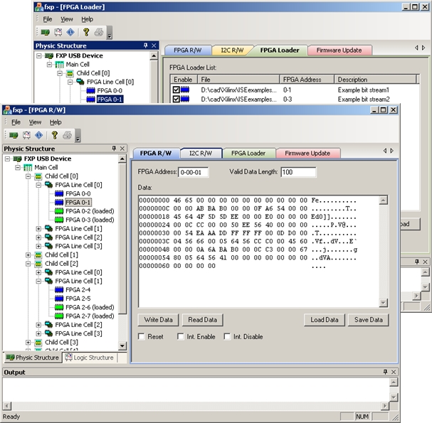
Program level is represented by the software package that includes:
- WDM Driver and interface description;
- User DLL pack;
- FXP MANAGER Application and user program modules interface;
FXP MANAGER Application provides two general tasks:
- Implementation of low-level protocol operations, system debugging. Application also supports TCL script language with extended set of commands, which simplify testing and debugging processes.
- Integration of the user program modules, which are intended for end-device operation.
The graphical user interface of the application is shown on figure 2.
Figure 2
Conclusion
FXP protocol is initially intended for utilization in large systems,
where its benefits are evident. For low-cost systems its modification - FXPL (FXP Lite) was developed.
The modifications were made only on the physical level,
so with relation to software - FXPLC provides the same set of features as FXP.
Application Notes
As the external interfaces of the protocol are completely specified,
there is no need to know the internal structure of the protocol
and how it works. For the practical use, it is suffice to copy
Reference Design, download drivers, controller firmware and DCU and
PBM bitstreams. In this case, we recommend purchasing of the FXPCTL
Evaluation Board that will help you while debugging and understanding the FXP protocol.
We wish you every success!
Development team of AdvanteX
|